Bathroom Fan Controller Circuit Diagram

Many bathrooms are fitted with a fan to vent  excess humidity while someone is showering. This fan can be connected to the light  switch, but then it runs even if you only want  to brush your teeth. A better solution is to  equip the fan with a humidity sensor. A disadvantage of this approach is that by the time  the humidity sensor switches on the fan, the  room is already too humid. Consequently, we decided to build a circuit  that operates by sensing the temperature of  the hot water line to the shower. The fan runs  as soon as the water line becomes hot. It continues to run for a few minutes after the line  cools down, so that you have considerably  fewer problems with humidity in the bathroom without having the fan run for no reason.

Naturally, this is only possible if you can  fit a temperature sensor somewhere on the  hot water line and the line does not become  warm if hot water is used somewhere else. We use an LM335 as the temperature sensor.  It generates an output voltage of 10 mV per  Kelvin. The output voltage is 3.03 V at 30 °C,  3.13 V at 40 °C, 3.23 V at 50 °C, and so on.  We want to have the fan switch on at a temperature somewhere between 40 and 50 °C (approx.100–150 °F). To do this accurately,we first use the opamps in IC2 to improve  the control range. Otherwise we would have  an unstable circuit because the voltage differences at the output of IC1 are relatively  small. IC2a subtracts a voltage of exactly 3.0 V from  the output voltage of IC1.

Bathroom Fan Controller Circuit Diagram


 Bathroom Fan Controller Circuit Diagram

It uses Zener diode  D1 for this purpose, so this is not dependent on the value of the supply voltage. The  value of R2 must be selected according to  the actual supply voltage so that the current through D1 is approximately 5 mA. It is  600 Ω with a 6-V supply (560 Ω is also okay),  or 2400 Ω (2.2 kΩ) with a 15-V supply. If you  have to choose between two values, use the  lower value. IC2b amplifies the output voltage of IC2a  by a factor of 16 ((R7 + R8) ÷ R8). As a result,  the voltage at the output of IC2b is 0.48 V at  30 °C, 2.08 V at 40 °C (104 °F), and 3.68 V at  50 °C (122 °F). Comparator IC3a compares this  voltage to a reference voltage set by P1. Due  to variations resulting from the tolerances of  the resistor values, the setting of P1 is best  determined experimentally. A voltage of 2.5 V  on the wiper should be a good starting point  (in theory, this corresponds to 42.6 °C).

When  the water line is warm enough, the output of IC3 goes Low. R10  provides  hysteresis  at  the  output  of  IC3a by pulling the voltage on the wiper of  the setting potentiometer down a bit when  the output of IC3a goes Low. IC3b acts as an  inverter so that relay Re1 is energised via T1,  which causes the fan to start running. After  the water line cools down, the relay is de-energised and the fan stops. If this happens  too quickly, you can reduce the value of R11  (to 33 kΩ, for example). This increases the  hysteresis. The circuit does not draw much current, and  the supply voltage is noncritical. A charging  adapter from a discarded mobile phone can  thus be used to power the circuit. If the supply voltage drops slightly when the relay is  energised, this will not create any problem.  In this case the voltage on the wiper of P1 will  also drop slightly, which provides a bit more  hysteresis on IC3a.

Author : Heino Peters - Copyright : Elektor
Read More

Call Bell with Welcome Indication Circuit Diagram

This is a simple call bell circuit that displays a welcome message when somebody presses the call bell switch momentarily. the alphanumeric display can be fitted near the call bell switch. the circuit is built around two 555 ICs (IC1 and IC2), seven KLA511 common-anode alphanumeric displays (DIS1 through DIS7) and a few discrete components. For easy understanding,  the entire circuit can be divided into  two sections: controller and display. the controller section is built around  IC1 and IC2, while the display section is built around alphanumeric displays (DIS1 through DIS7). 

As shown in the circuit, both IC1 and IC2 are wired as monostable  multivibrators having time periods of around 5 seconds and 2 minutes, respectively. You can change the time period of IC1 by changing the values of resistor R12 and capacitor  C3. Similarly, the time period of IC2  can be changed by changing the values of resistor R2 and capacitor C1. Alphanumeric displays DIS1 through DIS7 are wired such that they show ‘WELCOME’ when the output of IC2  goes high. the circuit is powered by a 6V battery. Else, you can use the 6V, 300mA power adaptor that is readily available in the market. the 6V battery or power adaptor provides regulated 6V required to operate the circuit. 

Call Bell with Welcome Indication Circuit Diagram


Call Bell with Welcome Indication Circuit Diagram

A 6V DC socket is used in the circuit to connect the output of the adaptor if you don’t use the battery. Working of the circuit is simple. First, power-on the circuit using switch S2. LED1 glows to indicate presence of power supply in the circuit. Now if you press call bell switch S1  momentarily, it triggers  both the timers (IC1 and  IC2) simultaneously. IC1 produces a high output at its pin 3 for about five seconds. transistor t2 conducts and piezobuzzer PZ1 sounds for about five seconds indicating that there is  somebody at the door. At the same time, IC2  too produces a high out-put at its pin 3 for about two minutes. transistor  t1 conducts to enable the alphanumeric displays. the word ‘WEL-COME’ is displayed  for about two minutes  as DIS1 through DIS7  ground via transistor T1.

If switch S1 is pressed again within these two minutes, piezobuzzer PZ1 again  sounds for five seconds and the display continues to show ‘WEL-COME’. Assemble the complete circuit on a general purpose PCB and house in a small cabinet with call bell switch S1 and LED1 mounted on the front panel. At the rear side of the cabinet, connect a DC socket for the adaptor. Install the complete unit (along with the display) at the entrance of your house. Connect the 6V battery or 6V adaptor for powering the circuit. Configure switch 2 (used to enable/disable the call bell) in a switch board at a suitable location inside your house. If you don’t use a battery, connect the power adaptor to the DC socket on the rear of the cabinet. Close switch S2 only when you want to activate the circuit with  battery. Otherwise, keep it open when the 6V adaptor is in use.

EFY note. 
1. To avoid any shorting  during rain, waterproof the entire circuit assembly including alphanumeric displays (installed at the entrance) by covering it properly.
2.  the complete kit for this circuit is available with EFY associates  kits’n’spares. 

Author : S.C. Dwivedi - Copyright : EFY
Read More

Simple Wireless Baby Monitor Project

This wireless baby monitor circuit using FM is designed to operate at a frequency of  100MHzefy tested. Its range of transmission is more than 100 metres with a 75cm wire antenna. The circuit is fully transistorised and so even a beginner can easily assemble it on a veroboard or the PCB whose pattern is given below for convenience.

Simple Wireless Baby Monitor Project


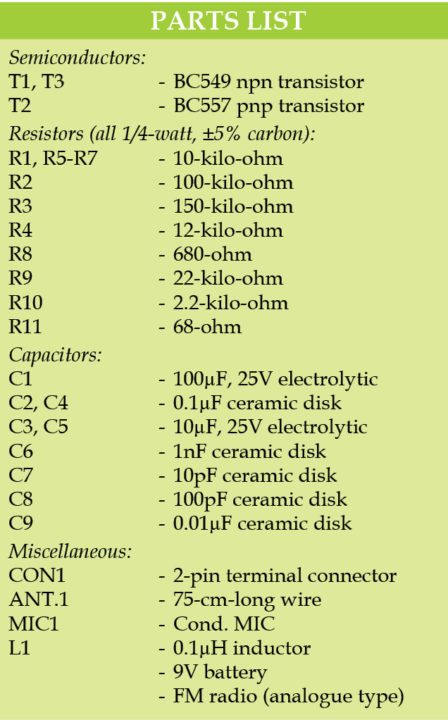
Circuit diagram of the wireless baby monitor circuit is shown in Fig. 1. It is built around a condenser microphone (MIC1), transistors BC549 (T1 and T3) and BC557 (T2), along with a few other components.

T1 and T2 provide high-gain audio to the VHF oscillator wired around T3. BC549 can oscillate well in VHF range. Frequency-modulated (FM) signals are transmitted through antenna ANT.1.

By adjusting trimmer capacitor VC1, frequency can be set within 88MHz -108MHz band. Using a good FM radio (analogue type) receiver, transmitted signals can be heard. Do not use a mobile phone as receiver.

This unit with 9-volt battery can be kept near a baby’s bed. Any sound generated by the baby including a cry can be monitored wirelessly from another room. Readily available 1-micro Henry inductor can be used as L1. It can also be home brewed as shown in Fig. 2.

Construction and testing

A single side PCB pattern of the wireless baby monitor circuit is shown in Fig. 3 and its component layout in Fig. 4. After assembling the circuit on a PCB, enclose it in a plastic case and keep it near the baby’s bed.


Read More

Simple Dog Whistle for Ronja Circuit Diagram

This is the Simple Dog Whistle for Ronja Circuit Diagram. Ronja is the author’s dog, a beagle-mongrel,  who seems increasingly often to need to be  called to heel either with a shout or with a  whistle. And so the idea came about for an  electronic dog whistle that could produce  two alternating high-frequency tones. A  design like this has several advantages over  conventional whistles or calling.
 
Circuit diagram :
Simple Dog Whistle for Ronja Circuit Diagram

Dog Whistle for Ronja Circuit Diagram
 
  • You can continue to carry on a conversation with your friends without having to  stop to whistle or call to your dog.
  • Using high frequencies means that  the whistle sound is barely audible to  (especially older) humans and so is less  annoying to other people than conventional whistles or calls. As is well known,  dogs have rather better hearing than  we do and can hear frequencies of up to  40 kHz.
  • The two alternating pitches mean that the  dog can more easily distinguish it from  other whistles.
 
The dog whistle is constructed from two  standard 555 timer ICs (or a single 556 IC),  both wired as astable multivibrators. The  first 555 oscillates at around 1.5 Hz and modulates the frequency of the second, which thus  switches between two different frequencies  every 0.7 seconds or so. The output of the second 555 is connected to a piezo sounder. If the  volume from the sounder used is insufficient, a small transistor amplifier can be added  between it and the output of the second 555. The circuit draws current only when activated by pressing S1. An optional green  LED indicates that the circuit is functioning.  When S2 is pressed the output frequencies  are reduced, making them more audible to  human ears for test purposes.
 
R1, R2 and C1 set the frequency of astable  multivibrator IC1. Diode D1 ensures that the  output is a symmetrical squarewave, by making C1 charge only via R1 and discharge only  via R2. Turning to IC2, where there is no diode in the  circuit, capacitor C2 is charged via R3 and R4  and discharged only via R4. With C2 = 22nF  the 555 oscillates at about 10 kHz; with S2  pressed, and hence C3 in parallel with C2, this  falls to about 1.8 kHz. Changing C2 to 10 nF  results in an even higher frequency (about  22 kHz), which can only be heard by dogs  and certain other animals. Setting C2 to 15 nF gives an output frequency of about 15 kHz. IC1 modulates the frequency of IC2 via R5. The green LED D2 is connected to the output  of IC1 via a series resistor and thus flashes at  the modulation frequency. The output from the piezo sounder at 10 kHz  (C2 = 22 nF) should be loud enough to verify  by ear. If desired, a more efficient piezo horn  tweeter can be used instead.


Author : Stefan Hoffmann
Read More

Novel Liquid-Level Sensor Circuit Diagram

Normally, the level of a liquid in a container is determined by sensing changes in the capacitance or resistance between a pair of electrodes that are immersed in the liquid. Generally speaking, this technique requires fairly complicated circuitry to protect the electrodes against electrolysis (and associated corrosion). In addition, in many cases the liquid must be conductive for the measurement principle to actually be usable. The circuit presented here shows that an alternative approach is possible.


Novel Liquid-Level Sensor Circuit Diagram

Here we utilise the fact that a PTC resistor warms up in pro-portion to the amount of current flowing through it, with the result that its resistance increases. If a PTC resistor is immersed in a liquid, the additional warmth is dissipated in the liquid and the resistance remains nearly constant.

 If the level of the liquid drops below the immersion depth of the resistor, the change in the resistance can be easily sensed by a subsequent comparator stage. The PTC resistor should be isolated from the fluid into which it is immersed, in order to prevent undesirable electrolytic processes from taking place. A further improvement in the characteristics of the circuit can be achieved by using a logic circuit such as a microcontroller to apply power to the circuit only at predefined times and then switch off the power after sampling the comparator output.


Read More

Heart Rate Monitor Circuit Diagram

Strictly speaking, this simple circuit shouldn't work! How could anyone expect an ordinary light dependent resistor photo cell to 'see' through a fingertip in natural daylight and detect the change in blood flow as the heart pulsates? The secret is a high gain circuit, based on a dual op amp IC which can be either the low power LM358 or the JFET TL072. The LDR is connected in series across the 9V battery supply via a 100kO resistor (R1) and the minute signal caused by the blood pulsing under the skin is fed to the non-inverting (+) input, pin 3, of IC1a via a 0.µF capacitor.

Pin 3 is biased by a high impedance voltage divider consisting of two 3.3MO resistors. The feedback resistors to pin 2 set the gain to 11 times. The output of IC1a is fed via a 0.47µF capacitor and 220kO resistor to IC1b. This is configured as an inverting op amp with a gain of 45 so that the total circuit gain is about 500. The output of IC1b is used to drive an analog meter which may be a multimeter set to the 10V DC range or any panel meter in series with a resistor to limit the current to less than its full-scale deflection. The prototype used an old VU meter with a 47kO resistor fitted in series.


heart-rate-monitor circuit diagram
Heart Rate Monitor Circuit Diagram

Note that the unit was designed to use the Dick Smith Electronics light dependent resistor (Z-4801). Other LDRs may require a change in the value of resistor R1. A light source such as a high brightness LED is not required. All that is needed is a reasonably well-lit room, preferably natural daylight, to produce a healthy swing of the needle. Only when the hands are very cold does it make it a little more difficult to accurately count the pulses. To check your heart rate, carefully position your thumb or finger over the LDR and count the meter fluctuations for a period of 15 seconds. Then multiply the result by four to obtain your pulse rate. The circuit can not be used if you are walking or running, etc.


Author: Tony Lee - Copyright: Silicon Chip Electronics Magazine
Read More

12V to 220V Inverter Circuit Diagram

Even though today’s electrical appliances are increasingly often self-powered, especially the portable ones you carry around when camping or holidaying in summer, you do still sometimes need a source of 230 V AC - and while we’re about it, why not at a frequency close to that of the mains? As long as the power required from such a source remains relatively low - here we’ve chosen 30 VA - it’s very easy to build an inverter with simple, cheap components that many electronics hobbyists may even already have.

Though it is possible to build a more powerful circuit, the complexity caused by the very heavy currents to be handled on the low-voltage side leads to circuits that would be out of place in this summer issue. Let’s not forget, for example, that just to get a meager 1 amp at 230 VAC, the battery primary side would have to handle more than 20 ADC!. The circuit diagram of our project is easy to follow. A classic 555 timer chip, identified as IC1, is configured as an astable multivibrator at a frequency close to 100 Hz, which can be adjusted accurately by means of potentiometer P1.


12V to 220V Inverter Circuit Diagram

 12V to 220V Inverter Circuit Diagram

As the mark/space ratio (duty factor) of the 555 output is a long way from being 1:1 (50%), it is used to drive a D-type flip-flop produced using a CMOS type 4013 IC. This produces perfect complementary square-wave signals (i.e. in antiphase) on its Q and Q outputs suitable for driving the output power transistors. As the output current available from the CMOS 4013 is very small, Darlington power transistors are used to arrive at the necessary output current. We have chosen MJ3001s from the now defunct Motorola (only as a semi-conductor manufacturer, of course!) which are cheap and readily available, but any equivalent power Darlington could be used.

These drive a 230 V to 2 × 9 V center-tapped transformer used ‘backwards’ to produce the 230 V output. The presence of the 230 VAC voltage is indicated by a neon light, while a VDR (voltage dependent resistor) type S10K250 or S07K250 clips off the spikes and surges that may appear at the transistor switching points. The output signal this circuit produces is approximately a square wave; only approximately, since it is somewhat distorted by passing through the transformer. Fortunately, it is suitable for the majority of electrical devices it is capable of supplying, whether they be light bulbs, small motors, or power supplies for electronic devices.

PCB layout:
pcb-layout-12-volt-to-230-volt-invertor-circuit-diagram
PCB Layout For Cheap 12V to 220V Inverter Circuit Diagram

COMPONENTS LIST
Resistors
R1 = 18k?
R2 = 3k3
R3 = 1k
R4,R5 = 1k?5
R6 = VDR S10K250 (or S07K250)
P1 = 100 k potentiometer
Capacitors
C1 = 330nF
C2 = 1000 µF 25V
Semiconductor
T1,T2 = MJ3001
IC1 = 555
IC2 = 4013
Miscellaneous
LA1 = neon light 230 V
F1 = fuse, 5A
TR1 = mains transformer, 2x9V 40VA (see text)
4 solder pins

Note that, even though the circuit is intended and designed for powering by a car battery, i.e. from 12 V, the transformer is specified with a 9 V primary. But at full power you need to allow for a voltage drop of around 3 V between the collector and emitter of the power transistors. This relatively high saturation voltage is in fact a ‘shortcoming’ common to all devices in Darlington configuration, which actually consists of two transistors in one case. We’re suggesting a PCB design to make it easy to construct this project; as the component overlay shows, the PCB only carries the low-power, low-voltage components.

The Darlington transistors should be fitted onto a finned anodized aluminum heat-sink using the standard insulating accessories of mica washers and shouldered washers, as their collectors are connected to the metal cans and would otherwise be short-circuited. An output power of 30 VA implies a current consumption of the order of 3 A from the 12 V battery at the ‘primary side’. So the wires connecting the collectors of the MJ3001s [1] T1 and T2 to the transformer primary, the emitters of T1 and T2 to the battery negative terminal, and the battery positive terminal to the transformer primary will need to have a minimum cross-sectional area of 2 mm2 so as to minimize voltage drop.

The transformer can be any 230 V to 2 × 9 V type, with an E/I iron core or toroidal, rated at around 40 VA. Properly constructed on the board shown here, the circuit should work at once, the only adjustment being to set the output to a frequency of 50 Hz with P1. You should keep in minds that the frequency stability of the 555 is fairly poor by today’s standards, so you shouldn’t rely on it to drive your radio-alarm correctly – but is such a device very useful or indeed desirable to have on holiday anyway? Watch out too for the fact that the output voltage of this inverter is just as dangerous as the mains from your domestic power sockets.
So you need to apply just the same safety rules! Also, the project should be enclosed in a sturdy ABS or diecast so no parts can be touched while in operation. The circuit should not be too difficult to adapt to other mains voltages or frequencies, for example 110 V, 115 V or 127 V, 60 Hz. The AC voltage requires a transformer with a different primary voltage (which here becomes the secondary), and the frequency, some adjusting of P1 and possibly minor changes to the values of timing components R1 and C1 on the 555.


Author : B. Broussas Copyright  Elektor Elecronics 2008
Read More

Simple Bicycle USB Charger Circuit Diagram

This is the Simple Bicycle USB Charger Circuit Diagram.This circuit has been developed to add a USB charging port to a bicycle for charging a mobile phone. The input supply for the circuit is produced by a dynamo (6V, 3W dynamo) in the bicycle. The circuit uses few components, which help in keeping the size, weight and cost of the unit down.


Circuit and working
The circuit is based on LM2596-5.0 (IC1). Its configuration, with minor changes, generally reflects the recommendations included in Texas Instruments’ datasheet of LM2596-5.0. The IC provides all active functions for a step-down (buck) switching regulator, capable of driving a 3A load with excellent line and load regulation.

The output of the regulator is 5V. It operates at a switching frequency of 150kHz, thus allowing smaller-sized filter components than what would be needed with traditional lower-frequency switching regulators. Fig. 1 shows the circuit diagram of the bicycle USB charger.


Fig. 1: Circuit diagram of the bicycle USB charger
 
The alternating voltage generated by the dynamo is converted to DC by a full-wave bridge rectifier comprising Schottky barrier rectifier diodes D1 through D4 and a filtering electrolytic capacitor (C1). The output of the bridge rectifier, which is charged to peak value of AC voltage (nearly 10V), is input to switching regulator LM2596-5.0 to provide a regulated 5V (DC) output, which is suitable for charging mobile devices using the USB connector.

The 5mm LED (LED1) in the circuit indicates output status. Feedback connection FB (pin 4 on IC1) is connected directly to output voltage at electrolytic capacitor C2. As with all switching regulators, C2 should have a low ESR (equivalent series resistance) rating. Besides, 33μH inductor (L1) should be rated for a DC current of at least 1A. The dynamo output is connected to the circuit by switch S1.

Construction and testing
An actual-size, single-side PCB of the bicycle USB charger is shown in Fig. 2 and its component layout in Fig. 3. Assemble the circuit on the PCB in such a way that you can connect the mobile phone through a USB connector.


Fig. 2: Actual-size PCB layout of the bicycle USB charger


Fig. 3: Component layout of the PCB

LM2596 (IC1) is available in a standard TO-220 package as well as in a surface mount TO-263 package. The PCB layout is for TO-220 package. The whole circuit can be easily constructed even on a perforated prototyping board. The USB output is soldered directly in the prototyping board. However, it is very important to observe correct polarity when connecting the USB output socket. After construction and testing, enclose the unit in a suitable ABS/acrylic box.


Sourced By :Streampowers
Read More

Automatic Plant Irrigator

The circuit presented here waters your plants regularly when you are out for a vacation. The circuit comprises a sensor part built using only one op-amp (N1) of quad op-amp IC LM324. Op-amp N1 is configured here as a comparator. Two stiff cop-per wires are inserted in the soil containing plants. As long as the soil is wet, conductivity is maintained and the circuit remains off. When the soil dries out, the resistance between the copper wires (sensor probes A and B) increases. If the resistance increases beyond a preset limit, output pin 1 of op-amp N1 goes ‘low’. 

Circuit diagram :
Automatic Plant Irrigator -Circuit -Diagram Automatic Plant Irrigator Circuit Diagram

This triggers timer IC2 (NE 555) configured as a monostable multivibrator. As a result, relay RL1 is activated for a preset time. The water pump starts immediately to supply water to the plants. As soon as the soil becomes sufficiently wet, the resistance between sensor probes decreases rapidly. This causes pin 1 of op-amp N1 to go ‘high’. LED1 glows to indicate the presence of adequate water in the soil. The threshold point at which the output of op-amp N1 goes ‘low’ can be changed with the help of preset VR1. To arrange the circuit, insert copper wires in the soil to a depth of about 2 cm,keeping them 3 cm apart. When the soil the water. LED1 glows up as the water reaches the probes.

For small areas a small pump such as the one used in air coolers is able to pump enough water within 5 to 6 seconds. The timing components for IC2 are selected accordingly. The timing can be varied with the help of preset VR2. The circuit is more effective indoors if one intends to use it for long periods. This is because the water from reservoir (bucket, etc) evaporates rapidly if it is kept in the open. For regulating the flow of water, either a tap can be used or one end of a rubber pipe can be blocked using Mseal compound, with holes punc-gets dried, adjust VR1 towards ground rail until LED1 turns off and relay RL1 is energised. The motor starts pumping tured along its length to water several plants.


Author: Priyank MudgaL - Copyright: Efymag
Read More

Fuel Reserve Indicator For Vehicles Circuit Diagram

Simple circuit for monitoring the fuel level in vehicles. It gives an audiovisual indication when the fuel level drops alarmingly below the reserve level, helping you to avoid running out of petrol on the way. Nowadays vehicles come with a dash-mounted fuel gauge meter that indicates the fuel levels on an analogue display. The ‘reserve’ level is indicated by a red marking in some vehicles, but the needle movement through the red marking may be confusing and not precise. This circuit monitors the fuel tank below the reserve level and warns through LED indicators and audible beeps when the danger level is approaching.


Fuel Reserve Indicator For Vehicles Circuit diagram
Fuel Reserve Indicator For Vehicles Circuit Diagram

The fuel sensor system consists of a tank-mounted float sensor and a current meter (fuel meter), which are connected in series. The float-driven sensor attached to an internal rheostat offers high resistance when the tank is empty. When the tank is full, the resistance decreases, allowing more current to pass through the meter to give a higher reading. The fuel monitoring circuit works by sensing the voltage variation developed across the meter and activates the beeper when the fuel tank is almost empty. Its point A is connected to the input terminal of the fuel meter and point B is connected to the body of the vehicle. The circuit consists of an op-amp IC CA3140 (IC1), two 555 timer ICs (IC2 and IC3) and decade counter CD4017 (IC4). 

Op-amp IC CA3140 is wired as a voltage comparator. Its inverting input (pin 2) receives a reference voltage controlled through VR1. The non-inverting input (pin 3) receives a variable voltage tapped from the input terminal of the fuel meter through resistor R1. When the voltage at pin 3 is higher han at pin 2, the output of IC1 goes high and the green LED (LED1) glows. This condition is maintained until the voltage at pin 3 drops below that at pin 2. When this happens, the output of IC1 swings from high to low, sending a low pulse to the trigger pin of the monostable (usually held high by R3) via C1. The monostable triggers and its output goes high for a predetermined time based on the values of R5 and C2. With the given values, the ‘on’ time will be around four minutes. 

The output of IC2 is used to power the astable circuit consisting of timer 555 (IC3) via diode D2. Oscillations of IC3 are controlled by R6, R7, VR2 and C4. With the given values, the ‘on’ and ‘off’ time periods are 27 and 18 seconds, respectively. The pulses from IC3 are given to the clock input (pin 14) of decade counter CD4017 (IC4) and its outputs go high one by one. When the circuit is switched on, LED1 and LED2 glow if your vehicle has sufficient petrol in the tank. 

When the fuel goes below the reserve level, the output of IC1 goes low, LED1 turns off and a negative triggering pulse is received at pin 2 of IC2. The output of IC2 goes high for around four minutes and during this time period, clock pin 14 of IC4 receives the clock pulse (low to high) from the output of IC3. For the first clock pulse, Q0 output of IC4 goes high and the green LED (LED2) glows for around 50 seconds. On receiving the second clock pulse, Q1 goes high to light up the yellow LED (LED3) and sound the buzzer for around 45 seconds. This audio-visual signal warns you that the vehicle is running out of fuel. On receiving the third clock pulse, LED3 and the buzzer go off. There is a gap of around two-and-a-half minutes before Q5 output goes high.

By the time Q5 goes high and the red LED (LED4) glows, four minutes elapse and the power supply to IC3 is cut off. The output state at Q5 will not change unless a low-to-high clock input is received at its pin 14. Thus LED4 will glow continuously along with the beep. The continuous glowing of the red LED (LED4) and the beep from the buzzer indicate that the vehicle will run out of fuel very shortly. Q6 output of IC4 is connected to its reset pin 15 via diode D3. This means that after ‘on’ state of Q5, the count will always start from Q0. Capacitor C5 provides power-on reset to IC4 when switch S1 is closed. The output of IC1 is also connected to reset pin of IC4 via diode D1 (1N4148). So when your vehicle is refueled above the reserve level, LED2 glows to indicate that the tank has sufficient fuel.

IC5 provides regulated 12V DC for proper functioning of the circuit even when the battery is charged to more than 12V. The circuit can be assembled on a perforated board. Adjust VR1 until the voltage at pin 2 of IC1 drops to 1.5V. When point A is connected to the fuel meter (fuel gauge) terminal that goes to the fuel sensor, green LEDs (LED1 and LED2) glow to indicate the normal fuel level. VR2 can be varied to set the ‘on’ time period of IC3 at around 20 seconds. Enclose the circuit in a small case and mount on the dashboard using adhesive tape. The circuit works only in vehicles with negative grounding of the body.


Author : D. Mohan Kumar
Read More

Dual High Side Switch Controller

One of the most frequent uses of n-channel MOSFET’s is as a voltage controlled switch. To ensure that the MOSFET delivers the full supply voltage to the load it is necessary for the gate voltage to be a few volts above the supply voltage level. This can be a problem if no other suitable higher volt-age sources are available for use elsewhere in the circuit. The LTC 1982 dual high-side switch controller from Lin-ear Technology (www.linear-tech.com) solves this problem by incorporating a voltage tripler circuit in the gate driver stage.

Circuit diagram :
Dual High-Side-Switch-Controller-Circuit-Diagram
Dual High Side Switch Controller Circuit Diagram


 The gate voltage is limited to +7.5 V which is 2.0 V above the IC’s maximum operating voltage. It can directly drive the gate of logic-level MOSFET with a VGS(th) from 1.0 V to 2.0 V. A suitable n-channel logic level MOSFET would be the BSP 295. This device can switch up to 1.5 A and is available in an SOT 233 SMD package.


Read More

Power-up/down Sequencer Circuit Diagram

Whether you’re talking about a home cinema  or a computer system, it’s very often the case  that the various elements of the system have  to be turned on or off in a quite specific order,  or at least, automatically. Constructing this  sort of automation system is well within the  capability of any electronics enthusiast worthy of the name, but in this ‘all-digital’ age,  most of the circuits of this type to be found  in amateur electronics magazines or web-sites use a microcontroller. Even though that  is indeed a logical solution (in  more ways than one!), and you  might even say the easiest one, it  does pose problems for all those  people who don’t (yet) have the  facilities for programming these  types  of  IC.  So  we  decided  to  offer you now an approach that’s  very different, as it only uses a  simple, cheap, commonly-avail-able analogue integrated circuit,  which of course doesn’t have to  be programmed. Our project in  fact uses as it’s ‘brain’ an LM3914,  a familiar IC from National Semiconductors,  usually  used  for  driving  LED  VU  (volume  unit)  meters. 

Circuit diagram :
Power-up-down Sequencer Circuitw
Power-up/down Sequencer Circuit Diagram

Before taking a look at the circuit  for  our  project,  let ’s  just  remind ourselves that the IC has  one analogue input and ten out-puts intended for driving LEDs.  It can operate in ‘point’ mode,  where the LEDs light up in turn,  from first to last, depending on  the input voltage, but only one LED is lit at  any given time. Alternatively  it can operate  in ‘bar’ mode (this is the mode normally used  for VU meters), and in this case, the LEDs light  up one after the other, in such a way as to create a strip of light (bar) that is longer or  shorter according to the input voltage. This is  the mode selected for the LM3914 in the circuit described in some detail below. 

So as to be able to control the AC powered equipment  our  sequencer  is  intended  to manage, we are using solid-state relays — four, in our example, though you can reduce or increase this number, up to a maximum of ten. Since the input devices in solid-state relays are LEDs, they can be driven directly by the LM3914 outputs, since that’s exactly what they’re designed for. As only four relays  are available, these are spread across out-puts L2, L4, L6, and L8, but you can choose  any arrangement you like to suit the number  of relays you want to use. 

Resistor R7 connected to pin 7 of the LM3914  sets the current fed to the LEDs by the LM3914  outputs. Here, it’s been set to 20 mA, since  that is the value expected by the solid-state  relays chosen. The input voltage applied to  pin 5 of the LM3914 is none other than the  voltage present across capacitor C1 — and  this is where the circuit is ingenious. When  the switch is set to ‘on’, C1 charges slowly  through R5, and the LEDs of the solid-state  relays on the outputs light one after another  as this voltage increases; in this way, the units  being controlled are powered up in the order you’ve chosen. To power-down, all you have  to do is flip the switch so that C1 discharges  through  R5,  and  the  LEDs  go  out  in  the  reverse order to that in which they were lit,  in turn powering down the units connected to the solid-state relays. Easy, isn’t it? If you’re not happy with the sequence speed,  all you need do is increase or reduce the  value of R5 in order to alter the speed one  way or the other.
The circuit needs to be powered from a volt-age of around 9 to 12 V, which doesn’t even  need to be stabilized. A simple ‘plug-top’,  ‘wall wart’ or ‘battery eliminator’ unit will be  perfect, just as long as it is capable of supply-ing enough current to power all the LEDs. As  the LED current is set by R7 to 20 mA per LED,  it’ll be easy for you to work out the current  required, according to the number of solid-state relays you’re using. 

In our prototype the type S216S02 relays  from Sharp were used, mainly because they  proved readily available by mail order. They also have the advantage of being compact,  and their switching capacity of 16 A means  you can dispense with a heatsink if you’re  using them for a computer or home cinema  system, where the current drawn by the vari-ous units can be expected to remain under  1 A. These solid-state relays must be protected by a fuse, the rating of which needs to  be selected according to the current drawn  by the devices being powered. 

Also note the presence across the relay terminals of a VDR, also known as a GeMOV or  SiOV, intended to protect them from any spurious voltage spikes. You can use any type  that ’s intended for operation on 250 VAC  without any problem. The values of fuses F1  to F4 are of course going to depend on the  load being protected. 

Construction of the circuit shouldn’t present any particular difficulty, but as the solid-state relays are connected directly to AC  power, it is essential to install it in a fully-insulated case; the case can also be used to  mount the power outlet sockets controlled  by the circuit. Note that sockets are female  components.
Let’s just end this description with the sole  restriction imposed by our circuit — but it’s  very easy to comply with, given the intended  use. In order to remain triggered, the solid-state relays must carry a minimum holding  current, which is 50 mA in the case of the  devices we’ve selected. In practical terms,  this just means that each of the devices powered by our sequencer must draw at least  50 mA, or in other words roughly 12 VA at  230 VAC, or 25 VA at 120 VAC.

Author :Christian Tavernier
Read More

Whistling Kettle Circuit Diagram

Most electric kettles do not produce a whistle and just switch off when they have boiled. Fitting a box of electronics directly onto an electric kettle (or even inside!) to detect when the kettle has boiled is obviously out of the question. The circuit shown here detects when the kettle switches off, which virtually all kettles do when the water has boiled. In this way, the electronics can be housed in a separate box so that no modification is required to the kettle. The box is prefer-ably a type incorporating a mains plug and socket. 

Cap

In this application, the current flowing in coil L1 provides a magnetic field that actuates reed switch S1. Since the current drawn by the kettle element is relatively large (typically 6 to 8 amps), the coil may consist of a few turns of wire around the reed switch. The reed switch is so fast it will actually follow the AC current flow through L1 and produce a 100-Hz buzz. The switching circuit driven by the reed switch must, therefore, disregard these short periods when the contacts open, and respond only when they remain open for a relatively long period when the kettle has switched off. 

Circuit diagram :
Whistling Kettle Circuit d
Whistling Kettle Circuit Diagram
 
The circuit is based on a simple voltage controlled oscillator formed around T2 and T3. Its operation is best understood by considering the circuit with junction R4/R5 at 0 V and C4 discharged. T2 will receive base current through R5 and turn on, causing T3 to turn on as well. The falling collector voltage of T3 is transmitted to the base of T2 by C4 causing this transistor to conduct harder. Since the action is regenerative, both transistors will turn on quickly and con-duct heavily. C4 will therefore charge quickly through T2’s base-emitter junction and T3. Once the voltage across C4 exceeds about 8.5 V (leaving less than 0.5 V across T2’s b-e junction), T2 will begin to turn off. This action is also regenerative so that soon both transistors are switched off and the collector volt-age of T3 rises rapidly to +9 V. With C4 still charged to 8.5 V, the base of T2 will rise to about 17.5 V holding T2 (and thus T3) off. C4 will now discharge relatively slowly via R5 until T2 again begins to conduct whereupon the cycle will repeat. The voltage at the collector of T3 will therefore be a series of short negative going pulses whose basic frequency will depend on the value of C4 and R5. The pulses will be reproduced in the piezo sounder as a tone. 

The oscillation frequency of the regenerative circuit is heavily dependent on the voltage at junction R4/R5. As this voltage increases, the frequency will fall until a point is reached when the oscillation stops altogether. With this in mind, the operation of the circuit around T1 can be considered. In the standby condition, when the kettle is off, S1 will be open so that C1 and C2 will be discharged and T1 will remain off so that the circuit will draw no current. When the kettle is switched on, S1 is closed, causing C1 and C2 to be discharged and T1 will remain off. C3 will remain discharged so that T2 and T3 will be off and only a small current will be drawn by R1. Although S1 will open periodically (at 100 Hz), the time constant of R1/C1 is such that C1 will have essentially no voltage on it as the S1 contacts continue to close. 

When the kettle switches off, S1 will be permanently open and C1/C2 will begin to charge via R1, causing T1 to switch on. C3 will then begin to charge via R4 and the falling voltage at junction R4/R5 will cause T2/T3 to start oscillating with a rising frequency. However, once T1 has switched off, C3 will no longer be charged via R4 and will begin to discharge via R3 and R5 causing the voltage at R4/R5 to rise again. The result is a falling frequency until the oscillator switches off, returning the circuit to its original condition. As well as reducing the current drawn by the circuit to zero, this mimics the action of a conventional whistling kettle, where the frequency rises as more steam is produced and then falls when it is taken off the boil. 

The circuit is powered directly by the mains using a ‘lossless’ capacitive mains dropper, C6, and zener a diode, D2, to provide a nominal 8 V dc supply for the circuit.  A 1-inch reed switch used in the prototype required about 9 turns of wire to operate with a 2-kW kettle element. Larger switches or lower current may require more turns. In general, the more turns you can fit on the reed switch, the better, but do remember that the wire has to be thick enough to carry the current. It is strongly recommended to test the circuit using a 9-volt battery instead of the mains-derived supply voltage shown in the circuit diagram. A magnet may be used to operate S1 and so simulate the switching of the kettle. 

Warning. This circuit is connected directly to the 230-V mains and none of the components must be touched when the circuit is in use. The circuit must be housed in an approved ABS case and carry the earth connection to the load as indicated. Connections and solder joints to components with a voltage greater than 200 volts across them (ac or dc) must have an insulating clearance of least 6 mm. An X2 class capacitor must be used in position C6.

Author :Bart Trepak
Read More

Battery-powered Night Lamp Circuit Diagram

This circuit is usable as a Night Lamp when a wall mains socket is not available to plug-in an ever running small neon lamp device. In order to ensure minimum battery consumption, one 1.5V cell is used, and a simple voltage doubler drives a pulsating ultra-bright LED: current drawing is less than 500µA.
An optional Photo resistor will switch-off the circuit in daylight or when room lamps illuminate, allowing further current economy.

This device will run for about 3 months continuously on an ordinary AA sized cell or for around 6 months on an alkaline type cell but, adding the Photo resistor circuitry, running time will be doubled or, very likely, triplicated.

Battery-powered Night Lamp Circuit Diagram

 Battery-powered Night Lamp Circuit diagram


Parts:
R1,R2___________1M   1/4W Resistors
R3_____________47K   1/4W Resistor (optional: see Notes)
R4____________Photo resistor (any type, optional: see Notes)

C1____________100nF  63V Polyester Capacitor
C2____________220µF  25V Electrolytic Capacitor

D1______________LED  Red 10mm. Ultra-bright (see Notes)
D2___________1N5819  40V 1A Schottky-barrier Diode (see Notes)

IC1____________7555 or TS555CN CMos Timer IC

B1_____________1.5V Battery (AA or AAA cell etc.)


Circuit operation:
IC1 generates a square wave at about 4Hz frequency. C2 & D2 form a voltage doubler, necessary to raise the battery voltage to a peak value able to drive the LED.

Notes:
  • IC1 must be a CMos type: only these devices can safely operate at 1.5V supply or less.
  • If you are not needing Photo resistor operation, omit R3 & R4 and connect pin 4 of IC1 to positive supply.
  • Ordinary LEDs can be used, but light intensity will be poor.
  • An ordinary 1N4148 type diode can be used instead of the 1N5819 Schottky-barrier type diode, but LED intensity will be reduced due to the higher voltage drop.
  • Any Schottky-barrier type diode can be used in place of the 1N5819, e.g. the BAT46, rated @ 100V 150mA.


Source :http://www.ecircuitslab.com
Read More

12 V Bidirectional Motor Control Circuit Diagram

This simple circuit drives DC motors with a maximum current of 1 A and can be built with readily available components.The output voltage is adjustable between 0 and 14 V and the polarity can be changed so that not only motor speed but also rotation direction can be adjusted by turning a knob. 

The circuit is also ideal as a controller for a DC model railway or small low voltage hobby tool. Power for the circuit is supplied by a 18 V mains transformer rated at 1.5 A. Diodes D1to D4 rectify the supply and capacitor C1 provides smoothing to give a DC output voltage of around 24 V. A classic ‘H’ bridge configuration is made up with transistors T1/T3 and T2/T4. Transistors T5 and T6 together with resistors R7 and R8 provide the current sense and limiting mechanism. The maximum output current limit can be changed from 1 A by using different value resistors for R7 and R8: IOUT = 0.6 V / R where R gives the value for R7 and R8. For increased current limit the mains transformer and diodes will need to be changed to cope with the extra current as well as the four transistors used in the bridge configuration. 

Circuit diagram:

12 V Bidirectional Motor Control Circuit Diagram

 12 V Bidirectional Motor Control Circuit Diagram
 
Motor speed control and direction is controlled by a twin-ganged linear pot (P1). The two tracks of P1 together with R1/R2 and R3/R4 form two adjustable potential divider networks. Wiring to the track ends are reversed so that as the pot is turned the output voltage of one potential divider increases while the other decreases and vice versa. 

In the midway position both dividers are at the same voltage so there is no potential difference and the motor is stationary. As the pot is rotated the potential difference across the motor increases and it runs faster. The voltage drop across D5 and D6 is equal to the forward voltage drop VBE of the bridge transistors and ensures that the motor does not oscillate in the off position with the pot at its mid point.
Read More

Water Pump Relay Controller Circuit Diagram

By means of a Relay, employed to drive a water pump, this circuit provides automatic level control of a water reservoir or well. The shorter steel rod is the "water high" sensor, whereas the longer is the "water low" sensor. When the water level is below both sensors, IC1C output (pin #10) is low; if the water becomes in contact with the longer sensor the output remains low until the shorter sensor is reached. At this point IC1C output goes high, Q1 conducts, the Relay is energized and the pump starts operating.

Now, the water level begins to decrease and the shorter sensor will be no longer in contact with the water, but IC1C output will be hold high by the signal return to pin #5 of IC1B, so the pump will continue its operation. But when the water level falls below the longer sensor, IC1C output goes low and the pump will stop. SW1 is optional and was added to provide reverse operation. Switching SW1 in order to connect R3 to pin #11 of IC1D, the pump will operate when the reservoir is nearly empty and will stop when the reservoir is full. In this case, the pump will be used to fill the reservoir and not to empty it as in the default operating mode.


Water Pump Relay Control Circuit Diagram

 Water Pump Relay Control Circuit Diagram


Parts:
R1 = 15K - 1/4W Resistors
R2 = 15K - 1/4W Resistors
R3 = 10K - 1/4W Resistor
R4 = 1K - 1/4W Resistor
D1 = LED - any type and color
D2 = 1N4148 - 75V 150mA Diode
Q1 = BC337 - 45V 800mA NPN Transistor
IC1 = 4001 Quad 2 Input NOR Gate CMos IC
SW = SPDT Toggle or Slide Switch (Optional)
RL1 = Relay with SPDT 2A @ 230V switch
Coil Voltage 12V - Coil resistance 200-300 Ohm
Two steel rods of appropriate length

Notes:
  • The two steel rods must be supported by a small insulated (wooden or plastic) board.
  • The circuit can be used also with non-metal tanks, provided a third steel rod having about the same height of the tank will be added and connected to the circuit's negative ground.


Read More

UV Torch Light Circuit Diagram

UV (ultra-violet) LEDs can produce eye-catching effects when their light is allowed to interfere with certain colours, particularly with reflected light under near-dark conditions. Also try shining some UV light on a diamond.

Circuit diagram :

UV Torch Light-Circuit Diagram
 UV Torch Light Circuit Diagram

Most UV LEDs require about 3.6 V (the ‘blue’ diode voltage) to light. Here, a MAX761 step-up switching IC is used to provide constant current to bias the UV diode. The IC employs PWM in high-cur-rent mode and automatically changes to PFM mode in low or medium power mode to save (battery) power. To allow it to be used with two AA cells, the MAX761 is configured in bootstrapped mode with voltage-adjustable feedback. Up to four cells may be used to power the circuit but they may add more weight than you would like for a torchlight. 

To prolong the switch life, R1 is connected to the IC’s SHDN (shutdown) pin. Less than 50 nA will be measured in shutdown mode. Electrolytic capacitor C1 is used to decouple the circuit supply voltage. With-out it, ripple and noise may cause instability. The one inductor in the circuit, L1, may have any value between about 10 and 50 µH. It stores current in its magnetic field while the MOSFET inside the MAX761 is switched. A toroid inductor is preferred in this position as it will guarantee low stray radiation. D1 has to be a relatively fast diode so don’t be tempted to use an 1N400x because it has a too slow recovery time.
The circuit efficiency was measured at about 70%. R2, the resistor on the feed-back pin of the MAX761 effectively determines the amount of constant current, I, sent through the UV LEDs, as follows: R2 = 1.5 / I
where I will be between 2 mA and 35 mA. 

Zener diode D4 clamps the output voltage when the load is disconnected, which may happen when one of the UV LEDs breaks down. Without a load, the MAX761 will switch L1 right up to the boost voltage and so destroy itself.

Author : Myo Min
Read More

Router UPS Circuit Diagram

It can be handy to have your phone and Internet router continue working for a while after  a power failure for example, if they provide  access to a security system. This requires a  backup power supply for the router. The version described here consists of a 12-V lead-acid battery and a voltage converter capable  of supplying an output voltage in the range of  15 to 30 V. It has built-in protection to prevent  excessive battery discharge.  This DIY uninterruptible power supply (UPS)  operates in standby mode as long as the  mains voltage is present. 


Router UPS-Circuit Diagram
Router UPS Circuit Diagram

The UPS consists of four parts: a backup  detector circuit that monitors the supply  voltage from the AC mains adapter, a battery  circuit that monitors the battery voltage to  prevent it from dropping below 11.8 V, a FET  switch between the battery and the voltage  converter, and a voltage doubler (inside the  dashed outline). To understand how it works, first consider  the situation with a router supply voltage  above 20 V, for which the voltage doubler is  not required. In this case the outputs of com-parators IC1a and IC1b (pins 1 and 7) are connected directly to the gate of the FET (G1 is  connected to G2). 

Under normal conditions the router, which is  connected to K3, is powered from the voltage  on connector K1. In this situation the voltage  on pin 2 of comparator IC1a is higher than 5.6  V. The output on pin 1 is therefore low, and  the FET is switched off. If the external volt-age on K1 drops out, the voltage on pin 2 of  IC1 drops and the output on pin 1 goes high,  switching on the FET. In this state the battery and the voltage converter supply power  to the router. The battery will gradually discharge, and to prevent the battery voltage  from dropping below 11.8 V the output of  the second comparator (on pin 7) goes low  when the voltage reaches this threshold level,  switching off the FET. The battery voltage  may rise quickly after the FET is switched off, so capacitor C3 is included to ensure that this  does not cause the FET be switched on again. 

Switch S1 allows the UPS to start up without an external supply voltage on K1, and capacitor C4 enables the comparators to continue operating in the event of a brief dropout of  the two supply voltages on K1 and K2. The emergency stop switch S2 and fuse F1 are included for safety reasons. The voltage converter has a high inrush current, so F1 must be generously dimensioned. 

If the router supply voltage is below 19 V, the  comparator output level in the high state is  too low to achieve a gate–source voltage of  4.5 to 5 V, since the source voltage is always  the same as the battery voltage under continuous charging, which is 13.8 V. This means  that the gate voltage must be at least 18.3 to  18.8 V, which is difficult or impossible with a  router supply voltage under 19 V. This can be  remedied by including the voltage doubler,  which is built around the well-known 555  timer IC (CMOS version). The frequency of the  oscillator (IC2) is approximately 40 kHz. Components C6, D5 and D6 add the AC voltage to  the switched supply voltage delivered by T2,  which is driven by the comparators in parallel  with the timer reset. An 18-V Zener diode (C7)  protects the FET gate–source junction against  overvoltage. 

Be careful to select a 555 with a maximum  rated supply voltage sufficient for this application; they are available in 16-V and 18-V  versions. The voltage converter of this UPS is a note-book power converter designed for in-car  use, with an input voltage of 12 V, selectable output voltage, and a minimum current  capacity of 0.5 A. Most voltage converters can  handle this easily. The battery must be connected to a good charger capable of maintaining a lead-acid battery in good condition  under prolonged no-load operation. Various  designs for this have been described in Elektor in the past. 

Adjust P1 for a voltage of approximately 7 V. With a lab power supply connected in place of the battery, adjust P2 for a threshold volt-age of 11.8 V.


Read More

Mobile Car Stereo Player Circuit Diagram

Using a mobile phone while driving is dangerous. It is also against the law. However, you can use your mobile phone as a powerful music player with the help of a stereo power amplifier. This does away with the need of a sophisticated in-dash car music system. Most mobile phones have a music player that offers a number of features including preset/manual sound equalisers. They have standard 3.5mm stereo sockets that allow music to be played through standard stereo headphones/sound amplifiers. Nokia 2700 classic is an example. 

Circuit diagram :

Circuit of mobile car stereo player
Mobile Car Stereo Player Circuit Diagram
 
A car audio amplifier with 3.5mm socket can be designed and simply connected to the mobile phone output via a shielded cable with suitable connectors/jacks (readymade 3.5mm male-to-male connector cable is a good alternative). Fig. 1 shows the circuit of car stereo player. It is built around popular single-chip audio power amplifier TDA1554Q (IC1). The TDA1554Q is an integrated class-B power amplifier in a 17-lead single-in-line (SIL) plastic power package. 

IC TDA1554Q contains four 11W identical amplifiers with differential input stages (two inverting and two non-inverting) and can be used for single-ended or bridge applications. The gain of each amplifier is fixed at 20 dB. Here it is configured as two 22W stereo bridge amplifiers. The amplifier is powered from the 12V car battery through RCA socket J2. Diode D1 protects against wrong-polarity connection. LED1 indicates the power status. 

Stereo Jack :
3.5mm stereo socket and (b) 3.5mm
(a) 3.5mm stereo socket and (b) 3.5mm Stereo Jack
 
Connect stereo sound signal from the 3.5mm headset socket of the mobile phone to audio input socket J1. When you play the music from your mobile, IC1 amplifies the input. The output of IC1 is fed to speakers LS1 and LS2 fitted at a suitable place in your car. Electrolytic capacitor C5 connected between pin 4 of IC1 and GND improves the supply-voltage ripple rejection. Components R2 and C4 connected at mute/standby pin (pin 14) of IC1 eliminate the switch on/off plop. The circuit is quite compact. A good-quality heat-sink assembly is crucial for IC1. Fig. 2 shows the stereo socket and stereo jack. 

Proposed enclosure Proposed enclosure

Assemble the circuit on a general-purpose PCB and enclose in a suitable cabinet. Small dimensions of the power amplifier make it suitable for being enclosed in a plastic (ABS) case with vent holes. Signal input socket, speaker output terminals, on/off switch, indicator, fuse holder and power supply socket are best located on the front panel of the enclosure as shown in Fig. 3. 


Author : T.K. Hareendran - Copyright : EFY
Read More

Fuse Failure Indicator Circuit Diagram

The indicator shows when the mains is present at its output by a continuous glow of a neon bulb, La1, and when the fuse is blown by flashing of the neon bulb. When the fuse is intact, capacitor C2 acts as the series resistance for the neon bulb, so that this glows continuously. When the fuse has blow, the mains voltage across diode D1 is applied as a pulsating direct voltage to network R1-C1. Capacitor C1 charges slowly and when the voltage across it reaches 80–100 V, the neon bulb comes on. Capacitor C1 is then discharged slowly via diode D2 and the bulb.

Circuit diagram :
fuse-failure-indicator-Circuit diagram
Mains/Fuse Failure Indicator Circuit Diagram

When the voltage across it has dropped sufficiently, the bulb goes out, whereupon C1 slowly charges again. This process repeats itself, so that, provided the values of R1 and C1 are right, the bulb flashes visibly. The potential across capacitor C2 is a ramp with a peak value of 30 V (which is, of course, applied to the load). Note that the neon bulb used for this purpose must not be a type that has a built-in series resistor.


Read More