12V to 220V Inverter Circuit Diagram

Even though today’s electrical appliances are increasingly often self-powered, especially the portable ones you carry around when camping or holidaying in summer, you do still sometimes need a source of 230 V AC - and while we’re about it, why not at a frequency close to that of the mains? As long as the power required from such a source remains relatively low - here we’ve chosen 30 VA - it’s very easy to build an inverter with simple, cheap components that many electronics hobbyists may even already have.

Though it is possible to build a more powerful circuit, the complexity caused by the very heavy currents to be handled on the low-voltage side leads to circuits that would be out of place in this summer issue. Let’s not forget, for example, that just to get a meager 1 amp at 230 VAC, the battery primary side would have to handle more than 20 ADC!. The circuit diagram of our project is easy to follow. A classic 555 timer chip, identified as IC1, is configured as an astable multivibrator at a frequency close to 100 Hz, which can be adjusted accurately by means of potentiometer P1.


12V to 220V Inverter Circuit Diagram

 12V to 220V Inverter Circuit Diagram

As the mark/space ratio (duty factor) of the 555 output is a long way from being 1:1 (50%), it is used to drive a D-type flip-flop produced using a CMOS type 4013 IC. This produces perfect complementary square-wave signals (i.e. in antiphase) on its Q and Q outputs suitable for driving the output power transistors. As the output current available from the CMOS 4013 is very small, Darlington power transistors are used to arrive at the necessary output current. We have chosen MJ3001s from the now defunct Motorola (only as a semi-conductor manufacturer, of course!) which are cheap and readily available, but any equivalent power Darlington could be used.

These drive a 230 V to 2 × 9 V center-tapped transformer used ‘backwards’ to produce the 230 V output. The presence of the 230 VAC voltage is indicated by a neon light, while a VDR (voltage dependent resistor) type S10K250 or S07K250 clips off the spikes and surges that may appear at the transistor switching points. The output signal this circuit produces is approximately a square wave; only approximately, since it is somewhat distorted by passing through the transformer. Fortunately, it is suitable for the majority of electrical devices it is capable of supplying, whether they be light bulbs, small motors, or power supplies for electronic devices.

PCB layout:
pcb-layout-12-volt-to-230-volt-invertor-circuit-diagram
PCB Layout For Cheap 12V to 220V Inverter Circuit Diagram

COMPONENTS LIST
Resistors
R1 = 18k?
R2 = 3k3
R3 = 1k
R4,R5 = 1k?5
R6 = VDR S10K250 (or S07K250)
P1 = 100 k potentiometer
Capacitors
C1 = 330nF
C2 = 1000 µF 25V
Semiconductor
T1,T2 = MJ3001
IC1 = 555
IC2 = 4013
Miscellaneous
LA1 = neon light 230 V
F1 = fuse, 5A
TR1 = mains transformer, 2x9V 40VA (see text)
4 solder pins

Note that, even though the circuit is intended and designed for powering by a car battery, i.e. from 12 V, the transformer is specified with a 9 V primary. But at full power you need to allow for a voltage drop of around 3 V between the collector and emitter of the power transistors. This relatively high saturation voltage is in fact a ‘shortcoming’ common to all devices in Darlington configuration, which actually consists of two transistors in one case. We’re suggesting a PCB design to make it easy to construct this project; as the component overlay shows, the PCB only carries the low-power, low-voltage components.

The Darlington transistors should be fitted onto a finned anodized aluminum heat-sink using the standard insulating accessories of mica washers and shouldered washers, as their collectors are connected to the metal cans and would otherwise be short-circuited. An output power of 30 VA implies a current consumption of the order of 3 A from the 12 V battery at the ‘primary side’. So the wires connecting the collectors of the MJ3001s [1] T1 and T2 to the transformer primary, the emitters of T1 and T2 to the battery negative terminal, and the battery positive terminal to the transformer primary will need to have a minimum cross-sectional area of 2 mm2 so as to minimize voltage drop.

The transformer can be any 230 V to 2 × 9 V type, with an E/I iron core or toroidal, rated at around 40 VA. Properly constructed on the board shown here, the circuit should work at once, the only adjustment being to set the output to a frequency of 50 Hz with P1. You should keep in minds that the frequency stability of the 555 is fairly poor by today’s standards, so you shouldn’t rely on it to drive your radio-alarm correctly – but is such a device very useful or indeed desirable to have on holiday anyway? Watch out too for the fact that the output voltage of this inverter is just as dangerous as the mains from your domestic power sockets.
So you need to apply just the same safety rules! Also, the project should be enclosed in a sturdy ABS or diecast so no parts can be touched while in operation. The circuit should not be too difficult to adapt to other mains voltages or frequencies, for example 110 V, 115 V or 127 V, 60 Hz. The AC voltage requires a transformer with a different primary voltage (which here becomes the secondary), and the frequency, some adjusting of P1 and possibly minor changes to the values of timing components R1 and C1 on the 555.


Author : B. Broussas Copyright  Elektor Elecronics 2008
Read More

3000 watt power inverter 12V DC to 230V AC

  3000 watt power inverter 12V DC  to  230V AC [link]

Circuit Diagram of 3000 watt power inverter 12V DC  to  230V AC
Circuit Diagram of 3000 watt power inverter 12V DC  to  230V AC


Fig. 2: Sine-wave voltage and conventional square wave voltage with both 230 Volt rms


Fig. 3: Square wave voltage with duty cycle 25% for 230 Volt rms ("modified sine")


PCB Layout:3000 watt power inverter 12V DC  to  230V AC
 
Component Placement: 3000 watt power inverter 12V DC  to  230V AC


fig.: output voltage with no load or inductive load.


fig.: resistor 0,001 Ohm made of high-grade steel sheet metal


Control electronics | 3000 watt power inverter 12V DC  to  230V AC

fig.: control electronics on strip hole plate (previous version) and PCB of the "professional edition"
Assembly of the mosfet-transistors on the heat sink | 3000 watt power inverter 12V   DC  to  230V AC


fig.: heat sink, mosfet transistors, connections.


Final assembly | 3000 watt power inverter 12V DC  to  230V AC

fig.: 1500 VA inverter with 2 parallel transformers and 1000 VA inverter

Source:qsl
Read More

Panasonic Microwave Oven Inverter HV Power Supply

Nearly all Panasonic microwave ovens now use an Inverter, and are always labelled with “Inverter” on
the front.

The High Voltage Power Supply Unit (HV PSU)
The HV PSU measures 165mm x 105mm x 60mm and weighs 650g.

 At left is the control daughter board. In front of that on the main board are the opto-isolators for the control and status signals brought out to the green connector. Back left is the rectified mains filter choke. The mains rectifier and switching transistors can just be seen on the heatsink behind the transformer. The mains filter capacitor is at right rear. The HV rectifiers and filters (doubler) are right front – white wires are the HV output from the transformer. The green wire is for grounding the HV +ve. The two lugs t right are for connecting HV -ve and heater to the magnetron. The winding thatcan be seen on the transformer is the primary and is made from 3mm finely stranded wire.

Here’s a view of the control end: 


This is the high voltage end:


The circuit for the HV PSU is below 

Notes about the circuit:
1. Apart from the block diagram, there is no information on the Inverter cont(o)rol circuit. The circuit itself is centred on one large, unmarked IC, so no help there.
2. The control and status signals seem to be a digital stream (2-3v suggestsa 5V data stream). They are opto-isolated because the majority of the circuit is at mains potential  (**BEWARE**). The part that isn’t is at 4kV (*** REALLY BEWARE ***)
3. The mains input side is monitored for both current and (under) voltage. No indication of what the control circuit does with this information.
4. The mains filter capacitor (C702) is very small – only 4uF. In a “normal” switching supply, there is usually 220 or 470 uF in this position.
5. Q701 that does all the hard work is a very heavy duty IGBT – a GT60N90 - 900V @ 60 A. Q702 forms some sort of flywheel circuit. This circuit from a Toshiba IGBT application note looks similar:


6. The HV side has a full-wave doubler rectifier and is marked 4kV @  300mA. Unlike the classic microwave oven transformers (where one side of the winding is grounded), this means that the secondary must be well insulated from ground on both sides. A simple reconfiguration of the rectifier (replace the caps with diodes) into a bridge circuit should yield 2kV @ 600mA (depending on the diode ratings)
7. The HV filter capacitors are only 8200 pF each, effectively giving 4100pF in the doubler. Considering that the inverter runs at about 30kHz, the reactance is equivalent to that  of a 5uF capacitor at 50Hz.
8. The positive side of the HV is grounded, so it’s a –4kV supply. Don’t simply swap the ground from the positive to the negative to get a +4kV supply, as the core of the transformer is also connected to this ground trace and will suddenly rise to 4kV above ground with disastrous and potentially fatal results. Instead, reverse the polarity of the rectifier diodes to get +4kV.


Source : By David Smith VK3HZ (vk3hz (*at*) wia.org.au)
Read More

230 Volt AC To Inverter Switching Circuit Diagram


Description

                  Before three weeks i am introduced  inverter circuit diagram but the circuit not included ac to inverter switching part so today i introducing a 230 Volt Ac to inverer switching circuit diagram .
Circuit showing a inverter switching  . Here i have used  bc 558 ,BC 548 and a relay for making this circuit . 230 volt connected to the base of the transistor Q1.When the power is ON positive volt coming to the base of the transistor so the relay circuit is open and load working in 230 V AC .When the power is OFF ground voltage coming to the base of the transistor so the Base of the Q2 is positive there for the   relay circuit closed and load working in inverter input .Part list and applications are showing below. 

Part List

Component No: Value  Usage
R1 100KΩ Emitter Load
R2 10K Ω Base Biasing 
R3180KΩ  Current Limiting 
Q1BC558  Switching  
Q2BC548   Switching 
D1 IN4007   Relay Balancing 
RL112 V  Inverter Switching 
Read More

DC to AC Inverter by IC 555 Circuit Diagram

This be basic AC inverter Circuit. Convenient for the initiator who have to is extremely fond of something experience. Because of use IC 555 highly popular, perform produce the frequency ,then enlarge with transistor NPN and PNP number TIP41 and TIP42 drive the coil transformer. Get by can pay Voltage output about 120V to 230V at frequency 50Hz. By have R4 perform control the frequency and should use. Voltage supply about 5V to 15V the detail sees in circuit picture sir. Link

 DC to AC Inverter by IC 555 Circuit Diagram

DC to AC Inverter by IC 555 Circuit Diagram

Read More

Toggle Touch Switch with Two Inverter Gates

Toggle Touch Switch with Two Inverter GatesYou can make a Toggle Touch Switch with Two Inverter Gates, two resistors, and two capacitors. The schematic diagram of the circuit is shown in the figure below. At power up, the output (of U1A) will be high, and the inverting output will be low because U1A gate will be triggered to ground level by C2. After triggered, the low level of U1A input is maintained by U1B output via R2.


If we touch the pad at this condition, where the output is high, then the U1A input will go high because we “short” the voltage of C1 to the input pin, and the low level previously caused by low level of U1B output voltage connected via R2 can’t be maintained because our skin resistance is much lower than 10M.

After U1A input goes high then U1A output will go low, and now U1B will go high to maintain high voltage level of U1A via R2, so we can release our finger without loosing the last state. Touching the pad again after we release our previous touching will toggle the output as the condition is reversed.

After we touch the pad, we have to release before 1 second (R2C2 time constant) elapsed. If we touch the pad longer than R2C2 time constant then  the output will oscillate (about 1 Hz).
Read More

Simple 12 to 120 Volt Inverter Circuit Diagram

This is the simple 12 to 120 Volt Inverter Circuit Diagram. Ever needed a low power 120volt AC power source for your car, van or truck? Well this circuit should do the trick for you. It will supply 15 watts of AC power to a device. It should power lamps, shavers, small stereos and small appliances. If you draw to much power the circuit will shut down all by itself. 

The output of this circuit is a square wave so there may be some noticeable hum on audio units plugged into it. To reduce some of the hum increase the value of the output capacitor which is at .47uf now. That transistor in the circuit are high power PNP transistors. Radio Shack part number 276-2025 are good ones to use or TIP32. The transformer is a 24 volt 2 amp center tapped secondary Radio Shack part number 273-1512 or equivalent. 

 12 to 120 Volt Inverter Circuit Diagram

12 to 120 Volt Inverter Circuit Diagram
Read More

1000W DC-AC Pure Sine Wave Power Inverter Circuit Diagram


DC-DC step-up part of the circuit RU190N08


Power circuit board


SPWM drive plate TDS2285 IC
Read More

110V-220V 500W or more inverter Circuit Diagram

110V-220V 500W or more inverter Circuit Diagram

i have constructed this inverter to charge my EV
i have 12V DC from solar pannels and i need to recharge my 120V battery pack so i needed an voltage inverter
after buying one i have tested it and it blowed in 2 hours
so i started building one myself using the ferite transformer and rewired it for my use
is very sinple and can be made for every one needs
can output any AC voltage with proper wiring
i use it only with 110v for my needs but in the diagram i had added another wiring for 110 and 120V

as you can see it powers an 200W halogen lamp for testing
in test i have used only 2 FETS but they are too hot so i have added another 2 for more power
if you use only 250W you can use only 2 with propper cooling
if you want more that 500W you need to add another 2 for every 250W of power and use an bigger transformer

from my findings this inverter has around 75% performance

Be carefull at output you have dangerous voltage

Step 1: The built inverter for 250W

110V-220V 500W or more inverter Circuit Diagram

110V-220V 500W or more inverter Circuit Diagram


As i said this one gets hotter with an 200W halogen lamp
if you want more power use more FETs and better transformer


DO NOT TRY MORE THAN 1000W is insane
for 250W you use 310W/12V=around 25A
for 500W you use 620W/12V=around 50A
for 750W you use 930W/12V=around 75A
for 1000W you use 1240W/12V=around 100A


Step 2:

DSC_0034.jpg
DSC_0032.jpg
DSC_0048.jpgDSC_0050.jpg

You can use an inverter to power your laptop from car batetry or use any house object that uses AC curent

This is the test inverter finished

I will post more pictures after i finish mounting it in its casing for car mounting

I have 240W solar panel on the roof of my car so i can charge my car any were is i have enough time

for DC you need to add an AC/DC rectifier and you can charge your EV battery ;)


BE CAREFUL YOU ARE PLAYING WITH DANGEROUS VOLTAGE

Read More

Inverter 5000 Watt PWM Circuit Diagram

This is a simple Inverter 5000 Watt PWM Circuit Diagram. This inverter uses PWM (Pulse Width Modulator) with type IC SG3524. IC serves as a oscillator 50Hz, as a regulator of the desired output voltage. Input power ranging from 250W up to 5000W output and has. Following a series INVERTER 5000W with PWM (Pulse Width Modulator).

 Inverter 5000 Watt PWM Circuit Diagram


Pcb Layout


Below is the output power settings that can be issued by this inverter:

DC voltage and Transformer "T2" winding recommendation:

Winding Power Supply

12VDC 750W P: 24V "12-0-12" / S: 220V

1500W 24VDC P: 48V "24-0-24" / S: 220V

2250w 36VDC P: 72V "36-0-36" / S: 220V

3000w 48VDC P: 96V "48-0-48" / S: 220V

3750w 60VDC P: 120V "60-0-60" / S: 220V

4500w 72VDC P: 144V "72-0-72" / S: 220V

5250w 84VDC P: 168V "84-0-84" / S: 220V


Transformer used is the transformer CT

R1 serves to regulate the voltage to 220v inverter

R2 serves to regulate the inverter output frequency of 50 or 60 Hz (as appropriate)

Read More

Voltage Inverter using IC NE 555 Circuit Diagram

In many circuits we need to generate an internal adjustable voltage. This circuit shows how it is possible to use a trusty old NE555 timer IC and a bit of external circuitry to create a voltage inverter and doubler. The input voltage to be doubled is fed in at connector K1. To generate the stepped-up output at connector K2 the timer IC drives a two-stage inverting charge pump circuit.

The NE555 is configured as an astable multivibrator and produces a rectangular wave at its output, with variable mark-space ratio and variable frequency. This results in timing capacitor C3 (see circuit diagram) being alternately charged and discharged; the voltage at pin 2 (THR) of the NE555 swings between one-third of the supply voltage and two-thirds of the supply voltage.


Voltage Inverter Circuit Using IC NE555 


The output of the NE555 is connected to two voltage inverters. The first inverter comprises C1, C2, D1 and D2. These components convert the rectangular wave signal into a nega-tive DC level at the upper pin of K2. The second inverter, comprising C4, C5, D3 and D4, is also driven from the output of IC1, but uses the negative output voltage present on diode D3 as its reference potential. The consequence is that at the lower pin of output connector K2 we obtain a negative volt-age double that on the upper pin.


Now let us look at the voltage feedback arrangement, which lets us adjust this doubled negative output voltage down to the level we want. The NE555 has a control voltage input on pin 5 (CV). Normally the voltage level on this pin is maintained at two-thirds of the supply voltage by internal circuitry. The voltage provides a reference for one of the comparators inside the device. If the reference voltage on the CV pin is raised towards the supply voltage by an external circuit, the timing capacitor C3 in the astable multivibrator will take longer to charge and to discharge. As a result the frequency of the rectangle wave output from IC1 will fall, and its mark-space ratio will also fall.

The source for the CV reference voltage in this circuit is the base-emitter junction of PNP transistor T1. If the base volt-age of T1 is approximately 500 mV lower than its emitter voltage, T1 will start to conduct and thus pull the voltage on the CV pin towards the positive supply.

In the feedback path NPN transistor T2 has the function of a voltage level shifter, being wired in common-base configuration. The threshold is set by the resistance of the feedback chain comprising resistor R3 and potentiometer P1. When the emitter voltage of transistor T2 is more than approximately 500 mV lower than its base voltage it will start to conduct. Its collector then acts as a current sink. Potentiometer P1 can be used to adjust the sensitivity of the negative feedback circuit and hence the final output voltage level.Using T1 as a voltage reference means that the circuit will adjust itself to compensate not only for changes in load at K2, but also for changes in the input supply voltage. If K2 is disconnected from the load the desired output voltage will be maintained, with the oscillation frequency falling to around 150 Hz.

A particular feature of this circuit is the somewhat unconventional way that the NE555’s discharge pin (pin 7) is connected to its output (pin 3). To understand how this trick works we need to inspect the innards of the IC. Both pins are outputs, driven by internal transistors with bases both connected (via separate base resistors) to the emitter of a further transistor. The collectors of the output transistors are thus isolated from one another [1].

The external wiring connecting pins 3 and 7 together means that the two transistors are operating in parallel: this roughly doubles the current that can be switched to ground.The two oscilloscope traces show how the output voltage behaves under different circumstances. The left-hand figure shows the behaviour of the circuit with an input voltage of 9 V and a resistive load of 470 Ω connected to the lower pin of output connector K2. The figure on the right shows the situation with an input voltage of 10 V and a load of 1 kΩ on the lower pin of output connector K2. The pulse width and frequency of the rectangle wave at the output of IC1 are automatically adjusted to compensate for the differing conditions by the feedback mechanism built around T1 and T2.

Because of the voltage drops across the Darlington out-put stage in the IC (2.5 V maximum) and the four diodes (700 mV each) the circuit achieves an efficiency at full load (470 Ω between the output and ground) of approximately 50 %; at lower loads (1 kΩ) the efficiency is about 65 %.


Author : Peter Krueger -  Copyright : Elektor
Read More

Simple Inverter Window Comparator Circuit Diagram

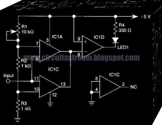
This is a simple Inverter Window Comparator Circuit Diagram ICl-c functions as a non inverting comparator, and ICl-a operates as an inverting comparator. Potentiometer Rl and fixed resistors R2 and R3 form a divider chain that delivers slightly different voltages to the two comparators. These voltages define the upper and lower limits of the circuit`s switching window, which can be changed easily by varying R2 and R3. The LED glows only when the input voltage falls within the window region.

Inverter Window Comparator Circuit Diagram


Inverter Window Comparator Circuit Diagram


Sourced By: Circuitsstream
Read More

USB 5V to 12V DC-DC Step-Up Converter by LT1618

This is a 5V to 12V DC-DC step-up (boost) converter circuitry that is especially ideal for the USB powered applications. First of all a USB port has two current supply modes. Before detecting the connected device, it supplies maximum 100mA to the load. After recognizing the device, it increases the output current up to 500mA. In this circuit, controller (LT1618) also provides two input current modes. 100mA and 500mA input modes can be selected by the user.

USB 5V to 12V DC-DC Step-Up Converter by LT1618 


USB 5V to 12V DC-DC Step-Up Converter by LT1618

Output currents are limited due to the increased potential difference at the output. When the demand of the load increases, output voltage will start to decrease. For example, if the circuit operates in the 100 mA input mode, when the load is 35 mA, the output voltage will be kept at 12V. But if the load increases to 50 mA, output voltage will reduce to 8V to maintain the constant 100 mA input current.
Read More

Simple Soldering Iron Inverter Circuit Diagram

This is a Simple Soldering Iron Inverter Circuit Diagram. This is a simple but inexpensive inverter for using a small soldering iron (25W, 35W, etc) In the absence of mains supply. It uses eight transistors and a few resistors and capacitors. Transistors Q1 and Q2 (each BC547) form an astable multivibrator that produces 50Hz signal. The complementary outputs from the collectors of transistors Q1 and Q2 are fed to pnp Darlington driver stages formed by transistor pairs Q3-Q5 and Q4-Q6 (utilising BC558 and BD140). The outputs from the drivers are fed to transistors Q7 and Q8 (each 2N3055) connected for push-pull operation.  Use suitable heat-sinks for transistors Q5 through Q8. A 230V AC primary to 12V-0-12V, 4.5A secondary transformer (T1) is used.


Soldering Iron Inverter Circuit Diagram


Soldering Iron Inverter Circuit

The centre-tapped terminal of the secondary of the transformer is connected to the battery (12V, 7Ah), while the other two terminals of the secondary are connected to the collectors of power transistors T7 and T8, respectively. When you power the circuit using switch S1, transformer X1 produces 230V AC at its primary terminal. This voltage can be used to heat your soldering iron. Assemble the circuit on a generalpurpose PCB and house in a suitable cabinet. Connect the battery and transformer with suitable current-carrying wires. On the front panel of the box, fit power switch S1 and a 3-pin socket for connecting the soldering iron. Note that the ratings of the battery, transistors T7 and T8, and transformer may vary as these all depend on the load (soldering iron).


Author : Sanjay Kumar
Read More

Mini Power Inverter Circuit Diagram

Even robot systems occasionally need a negative supply voltage for some purpose or other, and in this kind of application in particular there is a need for an effective circuit that does  not  make  greater demands  then  necessary in terms of current or space. If a low current 5 V supply is needed and only +5 V is available, a natural manufacturer to turn  to  is  Maxim,  and indeed in this case they do not let us down.The best known integrated  circuit made by this company is the MAX232, a level shifter for serial ports with an integrated charge pump that does not need an external inductor. 

Mini Power Inverter Project  image:

 
Mini Power Inverter Img
Simple Mini Power Inverter   

Along the same lines, although with a more stable output voltage and higher efficiency, is the MAX660. The device can ‘mirror’ any input voltage between 1.5 V and 5.5 V. With a 5 V input the output is typically –4.7 V with a load of 100 mA. Efficiency at 10 mA is around 96 % and at 100 mA is around 88 %. With an open-circuit output the IC draws a quiescent current of just 120 μA.There is little to say about the circuit itself. 

Mini Power Inverter Circuit diagram :
Simple Mini Power Inverter Circuit Diagram
 
The 0 Ω resistor on pin 1 selects the operating frequency. With R1 fitted, the circuit operates at 80 kHz; without it, at 10 kHz. The combination of L1 and C5 slightly reduces ripple on the output voltage; the choice of inductor is not as critical as it would be if it formed part of the switching circuit.Gerber files for the printed circuit board (which uses some SMD components) are available for download from the Elektor website, ref. 070279-11.zip. R1, C1 and C4 are 0603 SMDs and C3 is an SMD tantalum electrolytic capacitor. Either the MAX-660CSA or the MAX660M can be used; both come in SO8 packages. L1 is a 10 μH SMD inductor rated at 300 mA. 
Read More