Ultra Low Drop Linear Regulator Circuit Diagram

The circuit is a MOSFET based linear voltage regulator with a voltage drop of as low as 60 mV at 1 ampere. Drop of a fewer millivolts is possible with better MOSFETs having lower  RDS(on)  resistance. 

The circuit in Fig.1 uses 15V-0-15V secondary output from a step-down transformer and employs an n-channel MOSFET IRF540 to get the regulated 12V output from DC input, which could be as low as 12.06V. The gate drive voltage required for the MOSFET is generated using a voltage doubler circuit consisting of diodes D1 and D2 and capacitors C1 and C4. To turn the MOSFET fully on, the gate terminal should be around 10V above the source terminal which is connected to the output here. The voltage doubler feeds this voltage to the gate through resistor R1. Adjustable shunt regulator TL431 (IC2) is used here as an error amplifier, and it dynamically adjusts the gate voltage to maintain the regulation at the output.

Ultra Low Drop Linear Regulator Circuit Diagram

Ultra Low Drop Linear Regulator Circuit Fig-1 Circuit Fig.1

With adequate heatsink for the MOSFET, the circuit can provide up to 3A output at slightly elevated minimum voltage drop. Trimpot VR1 in the circuit is used for fine adjustment of the output voltage. Combination of capacitor C5 and resistor R2 provides error-amplifier compensation. 

The circuit is provided with a short-circuit crow-bar protection to guard the components against over stress during accidental short at the output. This crow-bar protection will work as follows: Under normal working conditions, the voltage across capacitor C3 will be 6.3V and diode D5 will be in the off state since it will be reverse-biased with the output voltage of 12V. However, during output short-circuit condition, the output will momentarily drop, causing D5 to conduct and the opto-triac MOC3011 (IC1) will get triggered, pulling down the gate voltage to ground, and thus limiting the output current. The circuit will remain latched in this state, and input voltage has to be switched off to reset the circuit. 

Ultra Low Drop Linear Regulator fig-2 Circuit Fig.2

The circuit shown in Fig.2 follows a similar scheme. It can be utilised when the regulator has to work from a DC rail in place of 15V-0-15V AC supply. The gate voltage here is generated using an LM555 charge pump circuit as follows: 

When 555 output is low, capacitor C2 will get charged through diode D1 to the input voltage. In the next half cycle, when the 555 output goes high, capacitor C3 will get charged to almost double the input voltage. The rest of the circuit works in a similar fashion as the circuit of Fig. 1. 

The above circuits will help reduce power-loss by allowing to keep input voltage range to the regulator low during initial design or even in existing circuits. This will keep the output regulated with relatively low input voltage compared to the conventional regulators. 

The minimum voltage drop can be further reduced using low RDS(on) MOSFETs or by paralleling them.

Read More

1.5 - 35 Volt DC Regulated Power Supply Circuit Diagram

Here is the circuit diagram of regulated power supply. It is a small power supply that provides a regulated voltage, adjustable between 1.5 and 35 volts at 1 ampere. This circuit is ready to use, you just need to add a suitable transformer. This circuit is thermal overload protected because the current limiter and thermal overload protection are included in the IC.

Picture of the circuit:
 1A 1.5 volt to 35 volt dc Regulated Power Supply Circuit Schematic
1A Regulated Power Supply Circuit Schematic
Circuit diagram:
 1A 1.5 volt to 35 volt dc Regulated Power Supply Circuit Diagram
1A Regulated Power Supply Circuit Diagram
Transformer selection chart:
  Transformer Selection Chart for 1A 1.5 volt to 35 volt dc Regulated Power Supply Circuit Diagram
Transformer selection Guide-Table For Power Supply
Parts:
IC = LM317
P1 = 4.7K
R1 = 120R
C1 = 100nF - 63V
C2 = 1uF - 35V
C3 = 10uF - 35V
C4 = 2200uF - 35V
D1-D4 = 1N4007

Features:
  • Just add a suitable transformer (see table)
  • Great to power your projects and save money on batteries
  • Suitable as an adjustable power supply for experiments
  • Control DC motors, low voltage light bulbs, …
Specifications :
  • Preset any voltage between 1.5 and 35V
  • Very low ripple (80dB rejection)
  • Short-circuit, thermal and overload protection
  • Max input voltage : 28VAC or 40VDC
  • Max dissipation : 15W (with heatsink)
  • Dimensions : 52x52mm (2.1” x 2.1”)
Technical Specifications
  • Input Voltage = 40Vdc max Transformer
  • Output Voltage = 1.5V to 35Vdc
  • Output Current = 1.5 Amps max.
  • Power Dissipation = 15W max (cooled)
Note:
  • It has not to be cooled if used for small powers. 28 Volt AC max is allowed for the input voltage.
Read More

Ceiling Fan Regulator- Motor Speed Control Circuit Diagram

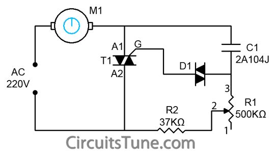
This is a simple ceiling fan regulator circuit diagram. It is used to control the speed of a ceiling fan. In the other words it is an AC motor speed controller circuit, as because it's control the speed of a AC motor(Ceiling Fan).  This ceiling fan regulator circuit built with few numbers of parts. The circuit mainly  based on Z0607 TRIAC. This is a low power AC semiconductor device. Generally which is used to controlling speed of low power ac motor speed. 

Circuit Diagram of Ceiling Fan Regulator :

Ceiling fan regulator-motor speed control circuit wiring diagram
Fig: Ceiling fan regulator circuit- AC motor speed controller 
In this ceiling fan regulator circuit, R1=500KΩ is a variable resistor that is used to adjust the fan speed. Capacitor C1 2A104J is a Polyester film capacitor.

Pin Diagram of  TRIAC(T1)- Z0607: 


Z0607 TRIAC Pin Diagram
Fig: Z0607-TRIAC Pin diagram

Pin Diagram of Variable Resistor R1:


Pin Diagram of Variable Resistor
Fig: Pin Diagram of Variable Resistor

Parts List Ceiling Fan Motor Speed Controller circuit:

T1 = Z0607 -TRIAC
D1 = DB3 C312 -DIAC
R1 = 500KΩ -Variable Resistor
R2 = 37KΩ -Resistor
C1 = 2A104J -Polyester film capacitor.
M1 = Single Phase AC Motor (Ceiling Fan)-220V,50Hz
Read More

Voltage Regulator Circuit Using LM317

The Voltage Regulator Circuit Using LM317 circuit diagram shows a way of powering a two-way mobile radio using the LM317T voltage regulator.

The LM317T is an adjustable 3-terminal positive voltage regulator that efficiently provides a load current of 1.5 Amps over an output range of 1.2 V and 37 V. With reference to the circuit, it can accept 14 volts without any hassle and the voltage can be controlled easily with the use of a potentiometer, a 3-terminal resister with sliding contact. The whole circuit will contain the following components:


Printed Circuit Board (PCB)
Resistor 1 (R1): 270 ohms
Resistor 2 (R2): 2K carbon potentiometer
Capacitor 1 (C1): 100nF
Capacitor 2 (C2): 1uF tantalum
LM317T Voltage Regulator
Heat Sink
DC Power Jacks
Green LED: Power
Red LED: Over Voltage
Zener Diode: over voltage LED switch

The zener diode switches on the over voltage LED if the voltage passing through is larger than the breakdown or preset voltage. The use of zener diode permits a constant amount of voltage and can be very beneficial for devices that inputs the same amount of voltage.

LM317T is cheaply available in the market and is very simple to integrate into several energy system to supply a maximum current or voltage
Read More

Monolithic Step-Down Switching Regulator Circuit Diagram

This is the Monolithic Step-Down Switching Regulator Circuit Diagram. L4962 is a monolithic step-down  switching regulator. It provides  output voltage of 5.1V to maxi-mum 40V, delivering current up to  1.2A to 1.5A, depending on the type  and package. The theoretical internal  functions are almost the same. The  heart  of  the  device  is  the  regulation  loop  consisting  of  a  saw  tooth  oscillator, error amplifier, comparator and  source-sink output stage.


 Fig. 1: Circuit of switching regulator

An error signal is produced by  comparing  the  output  voltage  with  a precise 5.1 volt on chip reference  (which is zener zap trimmed to ±2  per cent). This error signal is then  compared  with  the  saw  tooth  signal  to generate the fixed frequency pulse  width  modulated  pulses  which  drive the output stage.

Fig. 1 shows circuit diagram of  the regulator. The gain and frequency  of the loop can be set by RC network  connected to IC pin 11. When the loop  is  closed  directly  by  connecting  the  supply output to the feedback input  IC pin 10, an output voltage 5.1 volt is  produced. Higher output voltages are  obtained by inserting a voltage divider  in this feedback path. the outputs over current errors generated  at  the  on  switch  are  prevented  by  the  self-start  function.  The  error  amplifier  output is initially  clamped  by  the  external  capacitor ‘Css’ of pin15,  and  is  allowed  to  rise  linearly  as  this  capacitor  is  charged  by  a  constant  current  source.

Output overload protection is pro-vided in the from of a current limiter.  When the load current exceeds a preset  threshold, this comparator sets a flip-flop, which disables the output stage  and discharges the soft start capacitor. Another internal comparator resets  the flip-flop when the voltage across the soft capacitor C3 falls  to 0.4V. The output is thus  re-enabled  and  the  volt-age  rises  under  the  control of soft start network.  If overload condition is  still  present,  the  limiter  will  trigger  again  when  the  threshold  current  is  reached.  The  average  short-circuit is limited to a  safe value by the dead time introduced  in the soft start network. The thermal  overload circuit disables circuit operation when the junction temperature is  about 150°C and has hysteresis to  prevent instability. Frequency is about  100 KHz with parallel RC network connected to this terminal.

Specification
Fig. 2: Specification of L1 

Assemble the circuit on a general-purpose PCB by using two connectors one  for  the  input  and  the  other for the output. You can also use  a  DC-DC  converter  circuit  in  place  of  the  linear  regulator  to  avoid  the  use  of transformer and also to reduce dissipation. Finally, short-circuit protection is provided for all of the auxiliary  outputs by clips, internal current limiter and thermal protection circuit. The  specification of inductor L1 as shown  in Fig. 2. It is a ferrite torroid core T-18  with a small 20 turns of 27 SWG enameled copper wire. Sourced By : Link
Read More

Rotative Speed Regulator Borer, Driller Controller

This rotative speed regulator circuit schematic allows to control the holing speed of your borer or driller machine. This project is based on the fact that if the load grows, the voltage decrease and current increase. Use this circuit to control the speed of revolutions of your drilling mill or bench drill.

Driller controller circuit schematic

Circuit Project: Rotative speed regulator borer, driller controller 
Read More

Remote-Controlled Fan Regulator Circuit Diagram

Using this circuit, you can change the speed of the fan from your couch or bed. Infrared receiver module TSOP1738 is used to receive the infrared signal transmitted by remote control. The circuit is powered by regulated 9V. The AC mains is stepped down by transformer X1 to deliver a secondary output of 12V-0-12V. The transformer output is rectified by full-wave rectifier comprising diodes D1 and D2, filtered by capacitor C9 and regulated by 7809 regulator to provide 9V regulated output. Any button on the remote can be used for controlling the speed of the fan. Pulses from the IR receiver module are applied as a trigger signal to timer NE555 (IC1) via LED1 and resistor R4.

Remote-Controlled Fan Regulator Circuit Diagram

Remote-Controlled Fan Regulator Circuit Diagram

IC1 is wired as a monostable multivibrator to delay the clock given to decade counter-cum-driver IC CD4017 (IC2).Out of the ten outputs of decade counter IC2 (Q0 through Q9), only five (Q0 through Q4) are used to control the fan. Q5 output is not used, while Q6 output is used to reset the counter. Another NE555 timer (IC3) is also wired as a monostable multivibrator. Combination of one of the resistors R5 through R9 and capacitor C5 controls the pulse width.  The output from IC CD4017 (IC2) is applied to resistors R5 through R9. If Q0 is high capacitor C5 is charged through resistor R5, if Q1 is high capacitor C5 is charged through resistor R6, and so on.

Optocoupler MCT2E (IC5) is wired as a zero-crossing detector that supplies trigger pulses to monostable multivibrator IC3 during zero crossing. Opto-isolator MOC3021 (IC4) drives triac BT136. Resistor R13 (47-ohm) and capacitor C7 (0.01µF) combination is used as snubber network for triac1 (BT136). As the width of the pulse decreases, firing angle of the triac increases and speed of the fan also increases. Thus the speed of the fan increases when we press any button on the remote control. Assemble the circuit on a general-purpose PCB and house it in a small case such that the infrared sensor can easily receive the signal from the remote transmitter.


Sourced By:EFY
Read More

Low-drop Regulator with Indicator Circuit Diagram

This is an electronic Low-drop Regulator with Indicator Circuit Diagram. Even today much logic is still powered from 5 volts and it then seems obvious to power the circuit using a standard regulator from a rectangular 9-V battery. A disadvantage of this approach is that the capacity of a 9-V battery is rather low and the price is rather high. Even the NiMH revolution, which has resulted in considerably higher capacities of (pen-light) batteries, seems to have escaped the 9-V battery generation. It would be cheaper if 5 volts could be derived from 6 volts, for example. That would be 4 ‘normal’ cells or 5 NiMH- cells. Also the ‘old fashioned’ sealed lead- acid battery would be appropriate, or two lithium cells.
 
Low-drop Regulator with Indicator Circuit diagram :

Low-drop Regulator with Indicator-Circuit-Diagram
Low-drop Regulator with Indicator Circuit Diagram
 
Using an LP2951, such a power supply is easily realised. The LP2951 is an ever- green from National Semiconductor, which you will have encountered in numerous  Elektor Electronics designs already. This IC can deliver a maximum current of 100 mA at an input voltage of greater than 5.4 V. In addition to this particular version, there are also versions available for 3.3 and 3 V output, as well as an adjustable version.  In this design we have added a battery indicator, which also protects the battery from too deep a discharge. As soon as the IC has a problem with too low an input voltage, the ERROR output will go low and the regulator is turned off via IC2d, until a manual restart is provided with the RESET pushbutton.
 
The battery voltage is divided with a few resistors and compared with the reference voltage (1.23 V) of the regulator IC. To adapt the indicator for different voltages you only need to change the 100-k resistor. The comparator is an LP339. This is an energy-friendly version of the LM339. The LP339 consumes only 60 µA and can sink 30 mA at its output. You can also use the LM339, if you happen to have one around, but the current consumption in that case is 14 times higher (which, for that matter, is still less than 1 mA).
 
Finally, the LP2951 in the idle state, consumes about 100 µA and depend- ing on the output current to be deliv- ered, a little more. 

Author : Karel Walraven - Copyright : Elektor
Read More